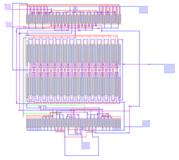
Fabricated PRSG die · probe-station bring-up at Carleton
Fabricated Silicon
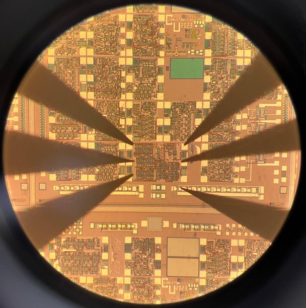
Custom CMOS IC: 31-Bit Pseudo-Random Sequence Generator
Full-custom CMOS · Carleton Microfab
5-STAGE FIBONACCI LFSR100% DRC/LVS CLEANFABRICATED & TESTED
Designed and fabricated a full-custom CMOS integrated circuit, laying out the design transistor by transistor from the ground up. The chip included five flip-flops configured as a Fibonacci linear feedback shift register, an XNOR feedback path for reset functionality, an on-chip RC oscillator to generate the clock signal, and a 10-mA output driver to push the signal off-chip.
The project was taken through the complete IC design flow, from schematic capture to a 100% DRC and LVS clean layout before fabrication at the Carleton University Microfab. After fabrication, the chip was tested on a probe station, and the measured hardware results were compared directly against simulation data to validate performance.